New year – New chip design
In 2023 we see an all-new series of flip chip in development projects for the first time at Check Point Group – A game changer for professional and industrial solutions.
The benefits of using the flip chip in high performance applications has been knownto us for quite some time, but the benefit of fitting them into new designs is a first in 2023.
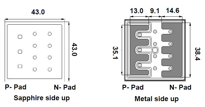
Performance and reliability are two main factors to why we now focus our attention towards the all new GaN series and first out for development is the 43-mil flip chip for UVA. The die size is 1092μm×11092μm and chip thickness of 150μm.
Better thermal properties
For thermal properties it has a great advantage over the vertical chip.
The integration of the substrate is seamless and therefor also has excellent thermal properties.
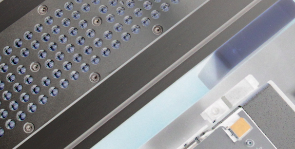
The bonding is, as it sounds flipped compared to the vertical chip and with the new series with the die face down. This allows for a strong bonding with die side down direct on substrate.
New bonding structure
The bonding wire is no longer in the design since the design uses conductive bonds. For 395nm industrial curing application this allows for a higher power with better heat distribution. The bonding is done with studs, solder or adhesives depending on the specific demands and volume in production for each project.
Higher reliability
Limited points of failure benefit all development projects, but particularly the COB – chip on board designs that we are focusing on for high performance industrial curing. As the traditional bond wire is a potential point of failure, we now have the possibility to eliminate completely. With designs containing flip chip, the elimination of traditional bonding methods creates a higher reliability.
More active surface
For UV-applications where optics are important for the curing result, we see that the flip chip also allows for a better product. Since the electrodes are located on the underside of the chip, it allows for the complete uniform upper surface to be UV-light emitting.
More active surface
For UV-applications where optics are important for the curing result, we see that the flip chip also allows for a better product. Since the electrodes are located on the underside of the chip, it allows for the complete uniform upper surface to be UV-light emitting.
Instant Active targeting
With instant response is it now possible to have a pulse curing, which means that for a short period of time start the curing process with a high energy boost, similar to bring the water up to the boiling point and thereafter reduce power – in order to finalize the curing. High intensity is achieved instantaneous and with pulse curing benefit it could greatly increase the performance and shorten curing time, even when comparing to a traditional UVA-vertical chip system.
Comparison to the HID-lamp is basically becoming irrelevant since the new and improved PI has a more defined target spectrum and with a PI responsive to 395-405nm we have ˃90% of the total power within the spectrum and over the threshold. Compared to a HID lamp the same reference value would be approx. ˂20% of the input energy that would be in the correct spectrum and over threshold.
New Design options
As a starting point for new designs in 2023 we go back to basics and start simulations in Ansys for heat distribution with the new chip series. For cooling options, we start with the basic forced convection and further evaluate liquid cooling. The forced convection with cold forged or extruded heatsinks are cost effective solutions for the industrial handheld market where liquid cooling is not an option due to weight limitations.
One step towards high performance industrial systems is the evaluation of liquid cooling for stationary systems. With liquid cooling the system is more complex, especially for risk management, but also highly rewarding from performance perspective.
Development loops
The complete design and optimization of lenses is also a key factor. In Synopsis LightTools, the process is simplified when analysing and optimizing the individual solution. It is a process of combining the design possibilities for the new flip chip and substrate, while keeping the customers target output in focus. The process of finding the optimal solution for a customer combines heat- and lens distribution. It usually takes a few development loops, both internal and external to find the most effective solution. A close relationship with tooling manufacturers for substrates, lenses and heatsinks is very valuable, since we more than often face new production challenges to meet the high customer demands.
C02 reduction is a key factor
Designing industrial and automotive manufacturers UV-curing as modular systems would be the next step for CO2-reduction since solution has huge cost saving potential with the cool curing UV-led systems. The systems would be operable at a fraction of the cost compared to traditional IR-systems
The modular system with flip chip technology has a way of controlling the industrial curing process that is unseen earlier.
– Both cost saving and CO2 reduction potential are extensive.
New Flip Chip series basics
- High brightness, long life
- 100% testing and sorting of chips
- Good consistency of wavelength and light intensity
- Die size: 43mil×43mil (1092±38μm×1092±38μm)
- Chip thickness: 5.9 mil (150 ± 15μm)
- P pad size: 35.1mil×13mil (892±15μm×330±15μm)
- N pad size: 38.4mil×14.6mil (976±15μm×372±15μm)